Extreme resolution 3D X-ray for advanced packaging
A commercial GPU with HBM is analysed using the Excillum NanoTube N3 X-ray source in a nanoCT setup.
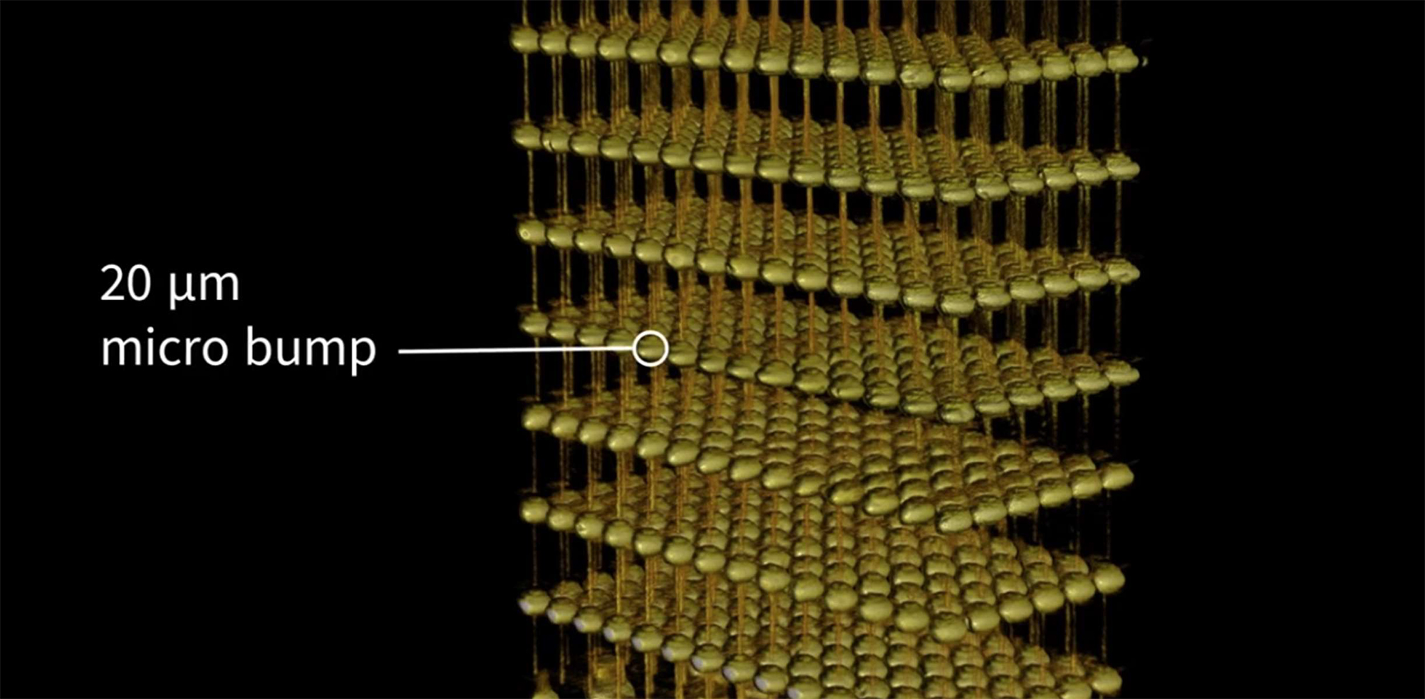
High Bandwidth Memory (HBM) micro bumps are used in advanced packaging in order to accommodate extremely fast data transfer between a GPU and HBM. The HBMs are stacked on top of each other close to the GPU and connected with Through Silicon Vias (TSV) and small (~20 µm) micro bumps. The process is expensive and each package has high value. It is therefore of high interest to be able to measure and detect e.g. alignment and shift of TSVs or shape and defects (voids, cracks, non-wetting, bulge missing bumps etc) in the micro bumps.
A slice through one of the planes filled with micro bumps connecting the memory dies show voids and defect such as deformation and cracks. Note that the smallest voids are less than 1 µm.


